Nvidia Unveils Custom NVHBM Architecture to Boost AI Accelerator Memory Bandwidth
The company's new memory framework relocates controllers to the 3D stack base die, offering lower power draw and greater die area for select NVLink Fusion partners.
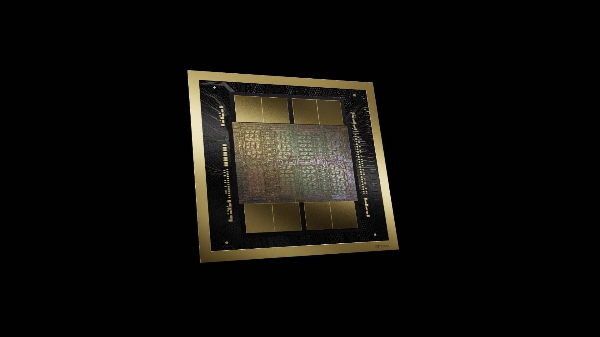
Nvidia has introduced a proprietary high-bandwidth memory design known as NVHBM, extending its NVLink Fusion initiative to tackle memory bandwidth constraints currently hindering frontier-level artificial intelligence workloads, as first reported by TechRadar Pro. The semiconductor giant unveiled the technology on August 26, outlining a framework engineered to increase data throughput, decrease power consumption, and recover valuable surface area on primary accelerator dies. Nvidia expects the custom memory architecture to enter high-volume production around 2027.
The performance projections published by Nvidia measure NVHBM against standard HBM4E test samples. According to company specifications, the architectural shift generates up to 30 percent higher memory bandwidth per individual memory stack while simultaneously cutting HBM power consumption by 15 percent. Additionally, the revised layout yields up to 25 percent more functional area on the underlying accelerator die. When benchmarked directly against the JEDEC HBM4E reference standard, Nvidia reported that NVHBM reduces the dedicated interface and support footprint by up to 67 percent.
Under existing industry norms, high-bandwidth memory design relies on a strict operational split between two distinct entities. Memory fabricators supply the dynamic random-access memory (DRAM) stack alongside its accompanying base die, whereas accelerator designers place the memory controller and physical interface on their own compute silicon. JEDEC standardizes the interconnect between these separate components, using a very wide but comparatively low-speed parallel bus to bridge the physical gap between the compute chip and memory stack.
NVHBM eliminates this traditional boundary by relocating Nvidia's custom memory controller directly into the base die of the three-dimensional memory stack. By transferring this function into the stack itself, Nvidia replaces the standard JEDEC parallel interface with a specialized, narrower serialized die-to-die interconnect. Nvidia supplies the design for this proprietary serialized link, enabling participating memory vendors to manufacture the integrated units directly.
The core concept of integrating memory control functions directly into the base die has previously surfaced in the enterprise hardware market. Marvell Technology announced a comparable architectural strategy in December 2024, partnering with key DRAM manufacturers Micron Technology, Samsung Electronics, and SK Hynix. At the time, Marvell reported that its custom approach yielded up to 25 percent more compute area, a 33 percent expansion in memory capacity, and a 70 percent reduction in memory interface energy demands. Contextualizing Nvidia's latest announcement, Counterpoint Research analyst Neil Shah stated, "The technology is not new. The distribution is."
Access to NVHBM will be tightly restricted through Nvidia's NVLink Fusion ecosystem, a strategic framework designed to integrate third-party compute accelerators into Nvidia's larger rack-scale server systems. Annapurna Labs, the custom silicon development arm of Amazon, has been named as the flagship partner involved in the broader NVLink Fusion expansion. Nvidia confirmed via a technical blog post that Annapurna will support NVLink Fusion within its upcoming Trainium4 processor lineup, though the company did not specifically identify Trainium4 as the direct recipient of the new NVHBM stacks.
The projected 2027 timeline means NVHBM will hit the market well after standard HBM4E configurations begin initial deployments. Leading memory producers are already moving toward HBM4E commercialization, with Samsung preparing to ship its first HBM4E engineering samples in late May 2026 and SK Hynix advancing its sampling schedule to approximately June 2026. Nvidia noted that NVHBM utilizes the same underlying building blocks slated for its future generation of graphics processing units, though it has not revealed which upcoming GPU family will be the first to feature the custom memory technology natively.
Sources
Written by
The Company Wire
Inside the companies building what’s next. Reporting on startups, technology, funding and the people shaping them.


