Samsung and TSMC Join Intel in Adopting ASML's $400M High NA Chipmaking Tools
Major semiconductor foundries are embracing ASML’s next-generation lithography tools and a new 12-inch photomask standard aimed at boosting production yields by 40 percent.
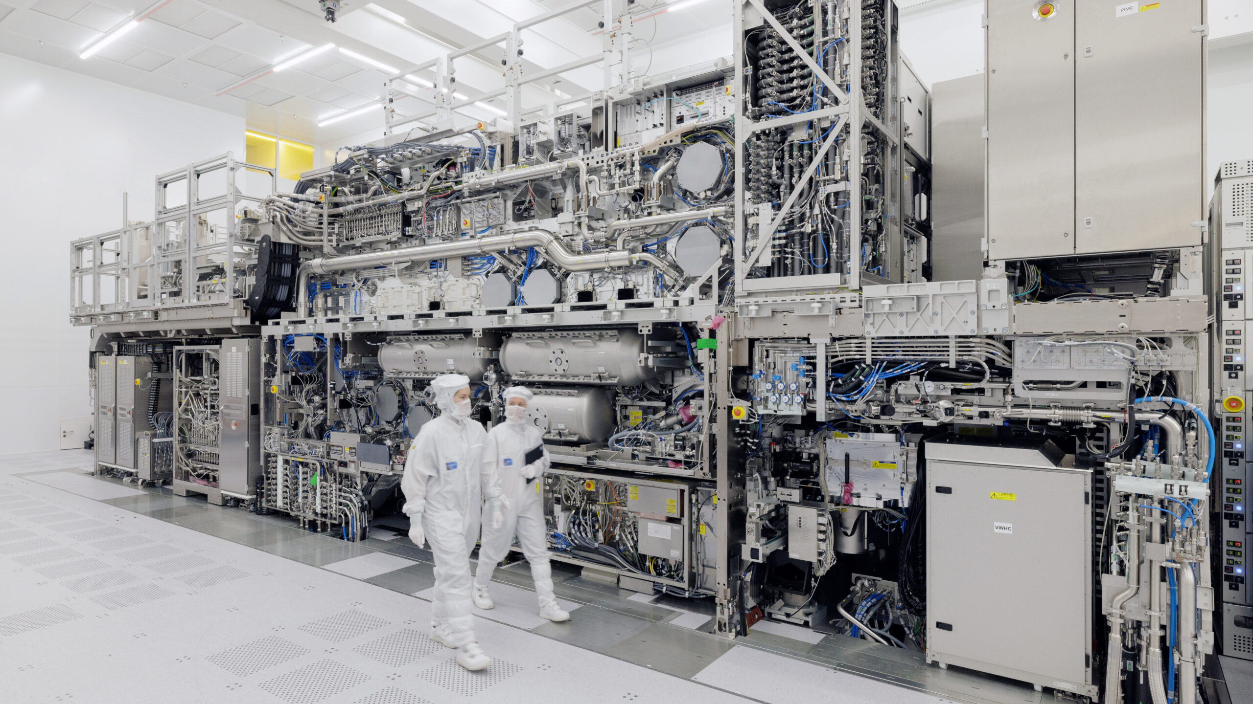
Samsung Electronics Co. and Taiwan Semiconductor Manufacturing Co. are committing to ASML Holding NV’s most advanced high-numerical-aperture lithography systems, joining Intel Corp. in backing a critical manufacturing change. As reported by Ars Technica, the major chipmakers have agreed to transition from 6-inch to 12-inch photomasks, a standardization shift that could boost output efficiency on ASML's $400 million machines by up to 40 percent.
The Dutch equipment giant stands as the world's sole supplier of extreme ultraviolet (EUV) photolithography scanners, which use laser light to etch intricate circuit patterns onto silicon wafers layer by layer. ASML’s newest high-numerical-aperture (high NA) EUV tools incorporate larger optical mirrors and refined optics to focus light with extreme precision, allowing chip designers to shrink feature sizes for next-generation artificial intelligence data centers and mobile devices.
To generate the required light wavelengths, ASML’s bus-sized tools rely on high-powered laser systems that pulse molten tin droplets into a plasma reaching temperatures of approximately 200,000 degrees Celsius. Specialized mirrors manufactured exclusively by Germany's Zeiss Group collect and redirect the resulting ultraviolet light to project circuitry patterns onto silicon.
Under the new adoption schedules, Samsung intends to integrate high NA EUV tools into its memory production lines by 2028. Fellow South Korean memory maker SK Hynix Inc. is targeting a similar 2028 timeline for high NA memory manufacturing and is evaluating whether to join the industry consortium guiding the 12-inch photomask transition, a company spokesperson told Bloomberg.
TSMC, the world’s dominant foundry, plans to roll out high NA EUV manufacturing by 2030 to build cutting-edge processors for clients such as Apple, Nvidia, AMD, and Qualcomm. Meanwhile, Intel has led the early implementation of the technology, using high NA EUV equipment for commercial volume production of its Panther Lake mobile processors starting in July 2026.
The core efficiency gain stems from expanding the photomask stencils used to imprint circuit patterns. ASML Chief Technology Officer Marco Pieters told Bloomberg that enlarging these stencils from 6 inches to 12 inches enables scanners to process larger silicon areas in a single exposure, directly driving the expected 40 percent boost in manufacturing productivity.
The manufacturing push arrives as sustained capital investment in AI data centers puts pressure on global semiconductor capacity, contributing to memory chip shortages that have elevated prices for smartphones, personal computers, and gaming hardware. Simultaneously, access to ASML's advanced tools remains a key flashpoint in US-China technological competition. Export restrictions imposed by Dutch regulators alongside American diplomatic pressure restrict ASML from delivering EUV equipment to Chinese foundries like Semiconductor Manufacturing International Corp., with an executive at Zeiss Group recently estimating that domestic Chinese firms would require at least 15 years to independently replicate EUV lithography systems.
Sources
Written by
The Company Wire
Inside the companies building what’s next. Reporting on startups, technology, funding and the people shaping them.